From MOSFETs to FinFETs - The Soft Error Scaling Trends
Dr. Indranil Chatterjee
Single-event effects (SEE) in semiconductor devices are caused when highly energetic particles present in the natural space environment (e.g., protons, neutrons, alpha particles, or other heavy ions) strike sensitive regions of a device. Depending on several factors, the particle strike may cause no observable effect, a transient disruption of circuit operations, a change of logic state, or even permanent damage to the device or integrated circuit (IC). Single-event induced errors have been a consistent reliability concern not only for space, but also for terrestrial electronic systems [1] . As CMOS technologies scale, the reduction of supply voltages and nodal capacitances lead to reduced critical charges (Qcrit) needed to corrupt the information stored at circuit nodes. On the other hand, with decreasing transistor sizes, and increased doping densities, charge collection areas (usually referred to as sensitive area) per transistor and charge-collection efficiencies decrease. All these factors also depend on the physical structure of a transistor. With the transition from planar to FinFET transistor structures at the 14/16-nm node, the focus has shifted to SE effects in FinFET technologies and how these effects differ from those for planar technologies [1-4] .
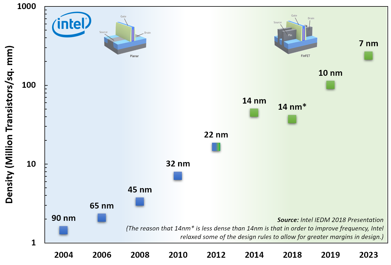
Figure 1: Packing density per chip across technology nodes.
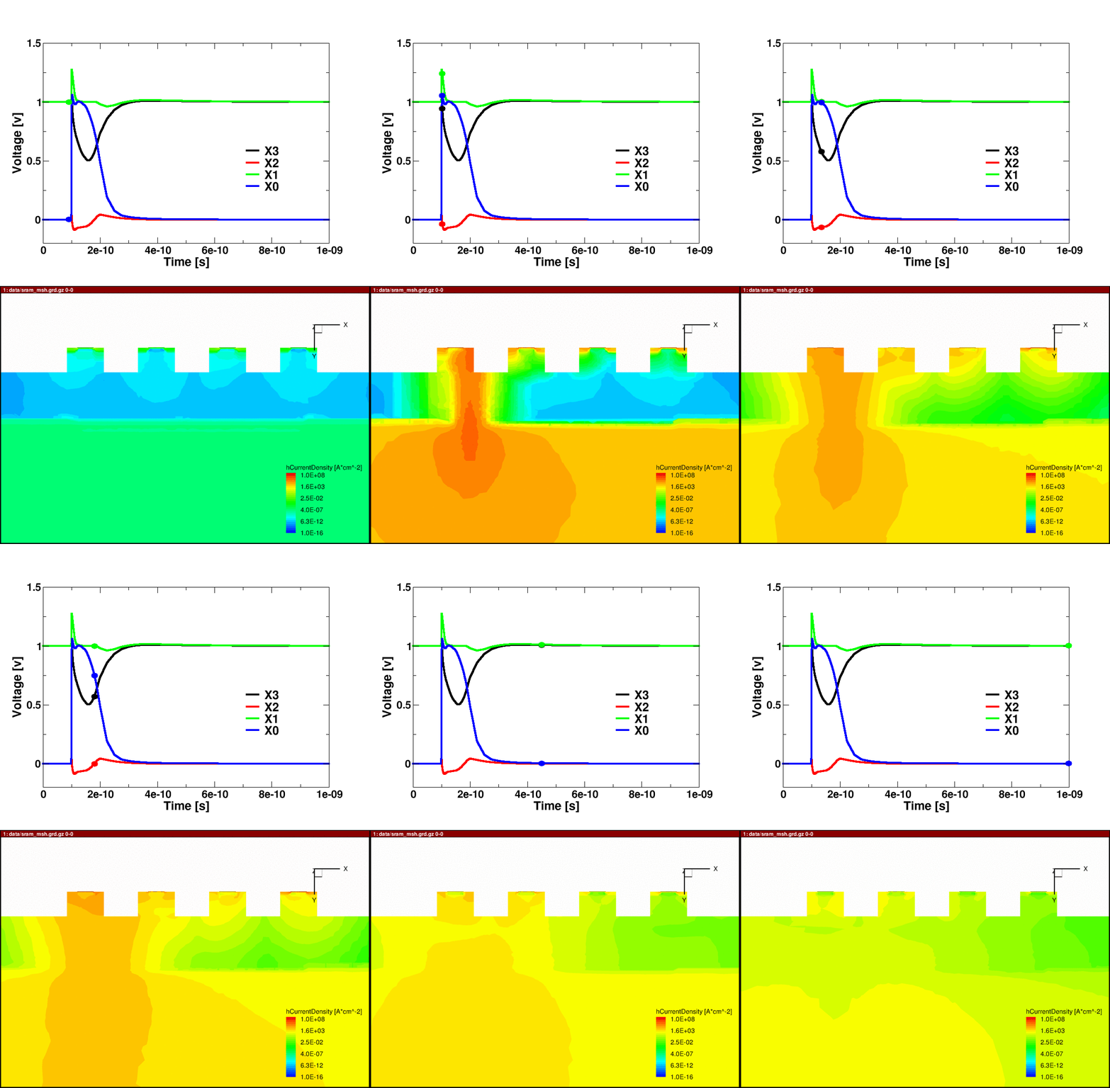
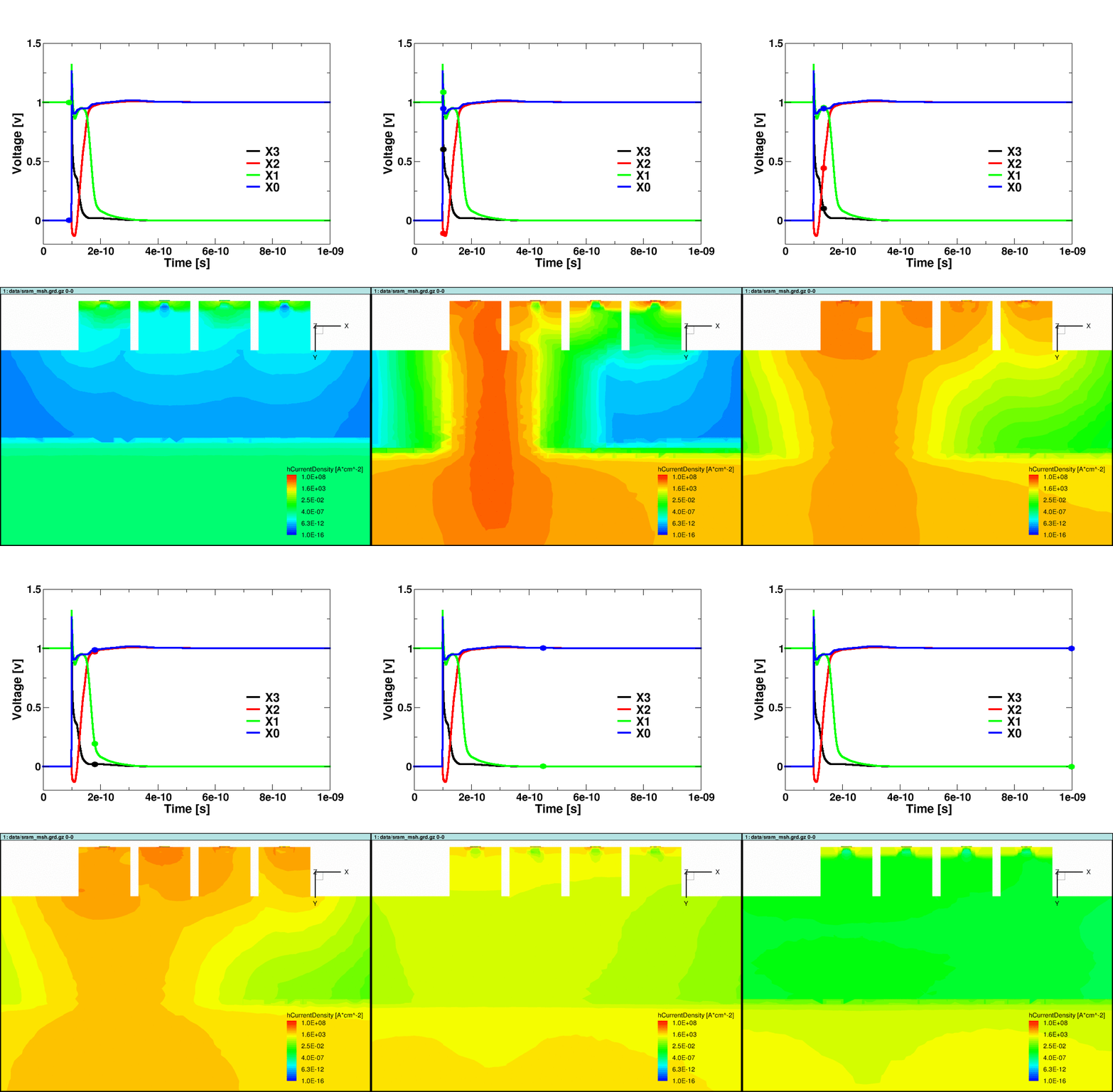
Figure 2: Ion strike in an SRAM in 45-nm and 20-nm technology node shows the significantly bigger impact on the smaller technology node. The charge cloud affects all transistors of the SRAM cell in the smaller technology node and causes the cell to upset. (Courtesy: Vanderbilt University)
Several works have been published over the years describing the soft error scaling trends across technology generations. It was observed that with each successive SRAM generation, the error per bit decreases. Also, reductions in charge collection efficiency due to shrinking depletion volume have been negated by significant reductions in operating voltage and thereby in nodal capacitance leading to lower critical charge (Qcrit) [5-6] . In the 1990’s and 2000’s operating speeds of digital circuits were steadily on the rise and billion transistor gate count was nearing. With increasing frequency of operation, an interesting prediction was that logic soft errors would be equal to, or even exceed flip-flop errors and become the dominant mechanism for errors in data path and control circuits [7] . As transistors got smaller, Dennard’s scaling law enabled chipmakers to ramp up the clock speed of their processors without increasing power consumption. However, in practice, device operating voltages have scaled less aggressively than the device dimensions. Thus, somewhere between 2005 and 2007, transistors became so small that increased current leakage caused to chips to overheat, which effectively prevented further clock speed-ups [8] . Circuit elements are broadly binned into two categories: storage cells (such as latches, flip-flops, and memories) and combinational logic circuits. Since logic circuit soft error rate (SER) strongly depend on operating frequencies (among other things), designers first identify the frequency at which logic SER will exceed latch SER. If the circuit operating frequency is beyond this frequency threshold then combinational logic errors may dominate system-level SER. On the other hand, if the operating frequency is below this threshold, memory and latch errors will be the dominant contributor towards the chip-level SER. For the past several technology nodes, most mitigation efforts have focused on protecting storage cells (memories and latches) because of their much larger contribution to overall soft error rates compared to that from logic circuits [9-11] . This was mainly because of the relatively low operating frequencies at which circuits were operated. Recent results at advanced technology nodes have shown that at the GHz range, logic SER may exceed memory SER [12-15] . However, as mentioned before, because of the limited scaling of operating voltages, the typical clock frequencies, nowadays, for CPUs are limited to 3.5 GHz, with 5.0 GHz pretty much the upper limit now. Thus, it would be interesting to observe how the contributions of various circuit elements to the system soft error rate stack up. For any electronic systems, memory, flipflop (FF), and logic soft error cross-sections are needed to evaluate the chip-level SE performance. This article presents a comprehensive picture of the SE scaling trends of memories, combinational and sequential circuit elements. Alpha particle exposures for combinational logic, latches, and memories fabricated in 45/40-nm, 32/28-nm, and 22/20-nm planar, and 14/16-nm bulk FinFET CMOS technology nodes are used to show the scaling trends. These trends are obtained using circuits that are representative of real-world data-path circuits, yielding results that can be extended to evaluate relevant chip-level SER for modern technology nodes, especially at high frequencies.
Memory Scaling Trends
Fig. 3 shows the single-event upset cross-section for the SRAM memory arrays for several technology nodes [12] , [15-18] . All the data points have been normalized to the SER observed for 40-nm SRAMs to allow direct comparison. Based on the number of events measured, the error bars for these data are less than 10% of the mean value across all technology nodes. As expected, the overall upset cross-section per bit decreases with technology scaling. While the first migration from planar to FinFET shows a large improvement in SER at nominal voltage, the subsequent scaling from 16 nm FinFET to 7 nm FinFET is shown to result in SER reduction proportional to the area scaling similar to SER trends observed within planar process nodes. SER for SRAMs depend on the critical charge (design dependent) and the amount of charge collected (fabrication process dependent) by a circuit node. The collected charge is influenced by charge confinement in the p-well after an ion strike. Subsequently, charge confinement is influenced by the well doping, which had increased with planar technology scaling to limit off-state leakage and threshold voltage manipulation. However, the isolation of the channel and better gate control in FinFETs allowed the well-doping to decrease in FinFET processes which in turn would increase charge sharing between transistors. Again, the narrow connection between the transistor and the bulk region for FinFETs diminishes charge-sharing effects [18] . If the extent of charge cloud were to be the same for FinFET node and planar node, one would expect the number of cells affected to increase by 9X for 16-nm node compared to 28-nm node (based on memory cell sizes [18] ). The proximity of cells and the decrease in critical charge for 16-nm node should result in increased MCU cluster size compared with 28-nm node for the same ion hit. However, the lower MCU contribution in 16-nm design implies less charge-sharing compared with planar processes. These results suggest that the charge collection efficiency has decreased significantly for FinFET technologies compared with planar technologies.
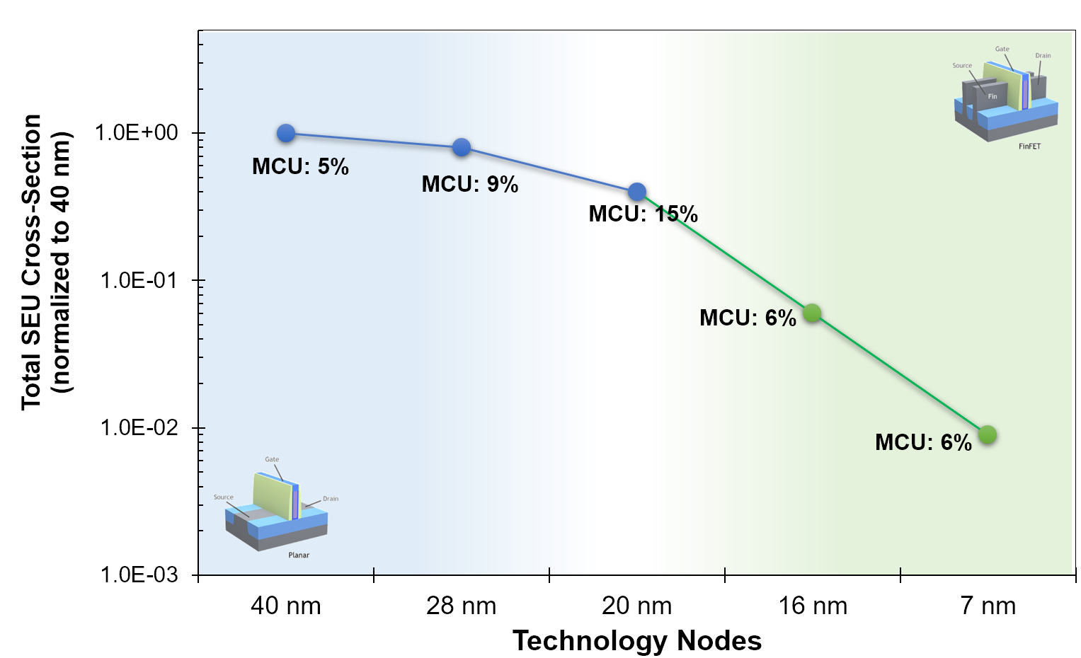
Figure 3: Normalized alpha particle induced SER as a function of technology for single-port SRAMs. The data labels indicate MCU rate as % overall SER.
Flip-flop and Logic Scaling Trends
Fig. 4 shows the ratio of the logic cross-section to FF cross-section for two frequencies (500 MHz and 1 GHz) across technology nodes (primary vertical axis) while the secondary vertical axis records the SE upset cross-section for standard DFF for various technology nodes [13] , [19-20] . The logic SE cross-section of 10 inverters was normalized by the latch SE cross-section at each technology node. It shows that the ratio of logic SE cross-section to FF cross-section decreases monotonically. An apparent anomaly in the scaling trends is the 20-nm node where the logic SE cross-section to latch SE cross-section ratio is higher than the 28-nm curve. This is primarily because the NMOS transistor widths in the 20-nm circuits were larger than those of the 28-nm NMOS transistor widths (in order to evaluate the relative impact of drain area). The larger NMOS transistors in 20-nm compared to 28-nm results in a marginally higher drive current that reduces the SET pulse-width, the product of the sensitive area of the drain and the SET pulse-width remains nearly same for these two technologies. In other words, the decrease in SET pulse-width due to scaling from 28-nm to 20-nm is compensated by the increase in area of the designed circuit. It is however crucial to note that the total SER at any given frequency decreases due to scaling, because both the latch and logic cross-sections decrease with scaling. But logic SER could become the dominant contributor to the total SER at much lower frequencies with scaling and with hardened latches, the frequency at which logic SER is higher than FF error would be lower. However, interestingly no logic errors were recorded for the 16-nm and 7-nm FinFET nodes up to 1.2 GHz. The reduced charge collection trends in FinFET processes compared to that of planar processes lead to very narrow transient pulse-widths which are possibly attenuated through the logic chain leading to almost no logic errors being recorded for alpha particle.
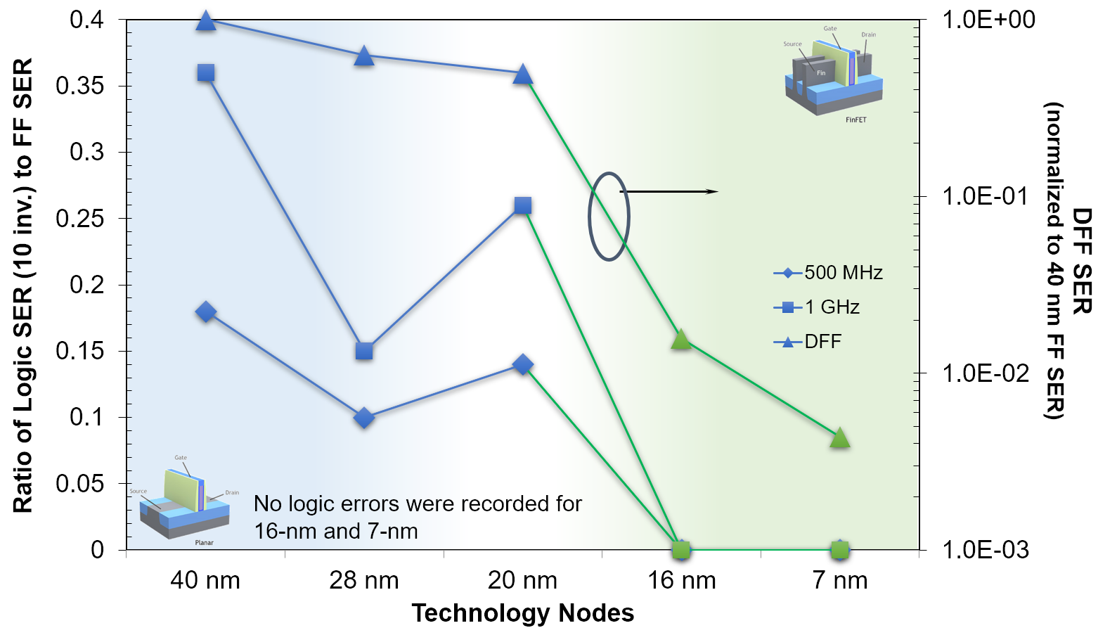
Figure 4: Normalized alpha particle induced SER as a function of technology for DFFs and ratio of logic error to FF errors for two different frequencies.
System level scaling trends
Fig. 5 shows the overall scaling trends for different types of circuits for alpha particles and heavy-ion exposures. As expected, these results show a declining trend with scaling. This shows that at nominal operating conditions, the system level SER trend is still dominated by latch SER by a significant margin. With the push to deploy high-speed on-board processing capability on satellites and interplanetary probes, logic SER will pose a significant hazard for space-based applications especially because almost all FF chains in space application deploy redundancy which would effectively lower the frequency threshold at which logic errors would become significant. But the scope of logic soft errors is unlikely to reach the levels predicted in 2002. Although the errors/bit is monotonically decreasing, soft errors are far from being insignificant when it comes to IC and system level FIT rate. With scaling, the cell size decreases, and critical charge needed to generate a given SET pulse width decreases. TCAD simulations show that the critical charge has decreased from 1.8 fC in 28-nm technology node to 0.9 fC in the 16-nm node for DFF [3] . Decreases in individual cell size reduce the probability that a given cell will be hit by an ion. Reduced critical charge increases sensitive region around an ion strike (cells further away from a hit location may still collect enough charge to cause an SET pulse). And on top of all these factors, scaling increases the total number of cells per given area. All these factors eventually result in similar number of upsets at the IC level across technology nodes (assuming comparable Si area per IC). With the increased system-level complexities (and the increased number of ICs to achieve these complex functions), the system-level error rates continues increase with each new generation.
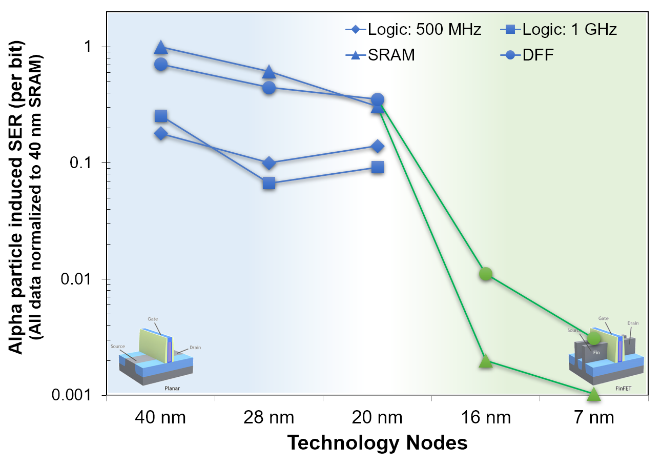
Figure 5: Overall scaling trend for memories, latches, and combinational logic for planar to FinFET technologies.
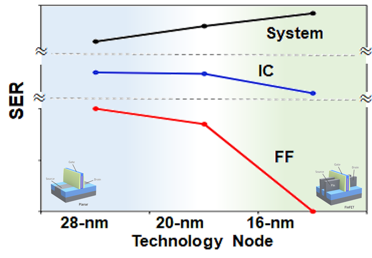
Figure 6: System level SER (empirical model).
Discussions
Technology scaling results in a reduction in the soft error cross-section for individual memory and latch bits as well as that for individual logic gates. However, the proportion of logic soft error cross-section to latch soft error cross-section for a given circuit depends on several parameters, such as frequency of operation, logic circuit size, topology, etc. At multi-GHz range of frequencies, potentially the logic error cross-section will be comparable to the latch SE cross-section and could exceed it as well. However, increased leakage current and chip overheating ensured that designed chips never managed to reach their frequency potential. Thus, the scope of logic soft errors is unlikely to reach the levels predicted at the turn of the century. However, increased number of cells per IC has resulted in almost constant soft error FIT rates across technology nodes. The introduction of 3D FinFET structure does show a slight decrease in chip-level SE FIT rates at the 16-nm node. However, increase system-level functionalities negate all these trends by requiring increased number of ICs at each successive generation. As we scale down to sub-5-nm technology nodes with Gate-All-Around (GAA) transistors, while interesting charge collection mechanisms may emerge, it is likely that the soft error vulnerability will continue to scale down at the bit level primarily because of the ever-decreasing charge collection volume. However, with increasing system-level complexity, as we move towards data-intensive, edge computing applications, system level soft errors are not going away with scaling.
References
- SIA Roadmap 2014
- Y-P. Fang and A. Oates, “Neutron-Induced Charge Collection Simulation of Bulk FinFET SRAMs Compared With Conventional Planar SRAMs”, IEEE Trans. Dev. and Mat. Reliab., Dec. 2011.
- P. Nsengiyumva, D. R. Ball, J. S. Kauppila, N. Tam, M. McCurdy, W. T. Holman, M. L. Alles, B. L. Bhuva, L. W. Massengill, ”A Comparison of the SEU Response of Plannar and FinFET D Flip-Flops at Advanced Technology Nodes”, IEEE Trans. Nucl. Sci., vol. 63, no. 1, pp. 266-272, Feb. 2016.
- N. Seifert, S. Jahinuzzaman, J. Velamala, R. Ascazubi, N. Patel, B. Gill, J. Basile, J. Hicks, ”Soft Error Rate Improvements in 14-nm Technology Featuring Second-Generation 3D Tri-Gate Transistors”, IEEE Trans. Nucl. Sci., vol. 62, pp. 2570-2577, Dec. 2015.
- R. Baumann, “The impact of technology scaling on soft error rate performance and limits to the efficacy of error correction,” Digest. International Electron Devices Meeting, San Francisco, CA, USA, 2002, pp. 329-332.
- R. Baumann, “Radiation-Induced Soft Errors in Advanced Semiconductor Technologies”, IEEE Trans. Dev. Mat. Rel., vol. 5, no. 3, pp.305-316, Sept. 2005.
- P. Shivakumar, M. Kistler, S. W. Keckler, D. Burger, and L. Alvisi, “Modeling the effect of technology trends on the soft error rate of combinational logic,” in Proc. IEEE Dependable Systems and Networks Conf. , Washington, DC, Jun. 2002, pp. 389-398.
- M. Feldman, “Dennard scaling demise puts permanent dent in supercomputing”, The Next Platform, June 2019.
- S. Mukherjee, J. Emer, S. K. Reinhardt, ”The soft error problem: an architectural perspective”, Proc. 11th International Symposium on High-Performance Computer Architecture, pp. 243-247, Feb. 2005.
- J. Maiz, S. Hareland, K. Zhang, P. Armstrong, ”Characterization of multi-bit soft error events in advanced SRAMs,” Proc. IEEE Electron Devices Meeting, pp. 21.4.1-21.4.4, Dec. 2003.
- P. Hazucha and C. Svensson, “Impact of CMOS technology scaling on the atmospheric neutron soft error rate”, IEEE Transactions on Nuclear Science, Vol 47, pp 2586-2594, Dec 2000.
- I. Chatterjee, B. Narasimham, N.N. Mahatme, B.L. Bhuva, R.A. Reed, R.D. Schrimpf, J.K. Wang, N. Vedula, B. Bartz, C. Monzel, “Impact of technology scaling on SRAM soft error rates”, IEEE Trans on Nucl. Sci., Vol 61, no. 6, pp 3512-3518, Dec 2014.
- N. N. Mahatme, I. Chatterjee N. J. Gaspard S. Jagannathan T. D. Loveless T. Assis B. L. Bhuva L. W. Massengill S. J. Wen, and R. Wong, ”Impact of technology scaling on combinational logic soft errors”, Proc. IEEE Int. Reliability Physics Symp., pp. 5.F.2.1-5.F.2.6 2014.
- B. Gill, N. Seifert, V. Zia, ”Comparison of alpha-particle and neutron-induced combinational and sequential logic error rates at the 32nm technology node,” Proc. IEEE Int. Rel. Phys. Symp., pp.199-205, 26-30 April 2009.
- N. Seifert, B. Gill, S. Jahinuzzaman, J. Basile, V. Ambrose, Quan Shi, R. Allmon, A. Bramnik, A., ”Soft Error Susceptibilities of 22 nm Tri-Gate Devices,” IEEE Trans. on Nucl. Sci., vol.59, no.6, pp.2666,2673, Dec. 2012.
- I. Chatterjee, B. Narasimham, N.N. Mahatme, B.L. Bhuva, R.D. Schrimpf, J.K. Wang, B. Bartz, E. Pitta, M. Buer, ”Single-Event Charge Collection and Upset in 40-nm Dual-and Triple-Well Bulk CMOS SRAMs”, IEEE Trans. Nucl. Sci., vol. 58, no. 6, pp.2761-2767, Dec. 2011.
- B. L. Bhuva, N. Tam, L. W. Massengill, D. Ball, I. Chatterjee, M. McCurdy, M. L. Alles, ”Multi-Cell Soft Errors at Advanced Technology Nodes”, IEEE Transactions on Nuclear Science, vol. 62, pp. 2585-2591, 2015.
- B. Narasimham, S, Gupta, D. Reed, J. K. Wang, N. Hendrickson, H. Taufique, “Scaling trends and bias dependence of the soft error rate of 16 nm and 7 nm FinFET SRAMs”, Proc. IEEE Int. Rel. Phys. Symp., May 2018.
- H. Jiang, H. Zhang, R. C. Harrington, J. A. Maharrey, J. S. Kauppila, L. W. Massengill, B. L. Bhuva, “Impact of supply voltage and particle LET on the soft error rate of logic circuits”, Proc. IEEE Int. Rel. Phys. Symp., May 2018.
- J. Cao; L. Xu; B. L. Bhuva; S. -J. Wen; R. Wong; B. Narasimham; L. W. Massengill, “Alpha Particle Soft-Error Rates for D-FF Designs in 16-Nm and 7-Nm Bulk FinFET Technologies”, Proc. IEEE Int. Rel. Phys. Symp., May 2019.